

Arduino
Arduino Nano 33 BLE
Arduino Nano 33 BLE
Couldn't load pickup availability
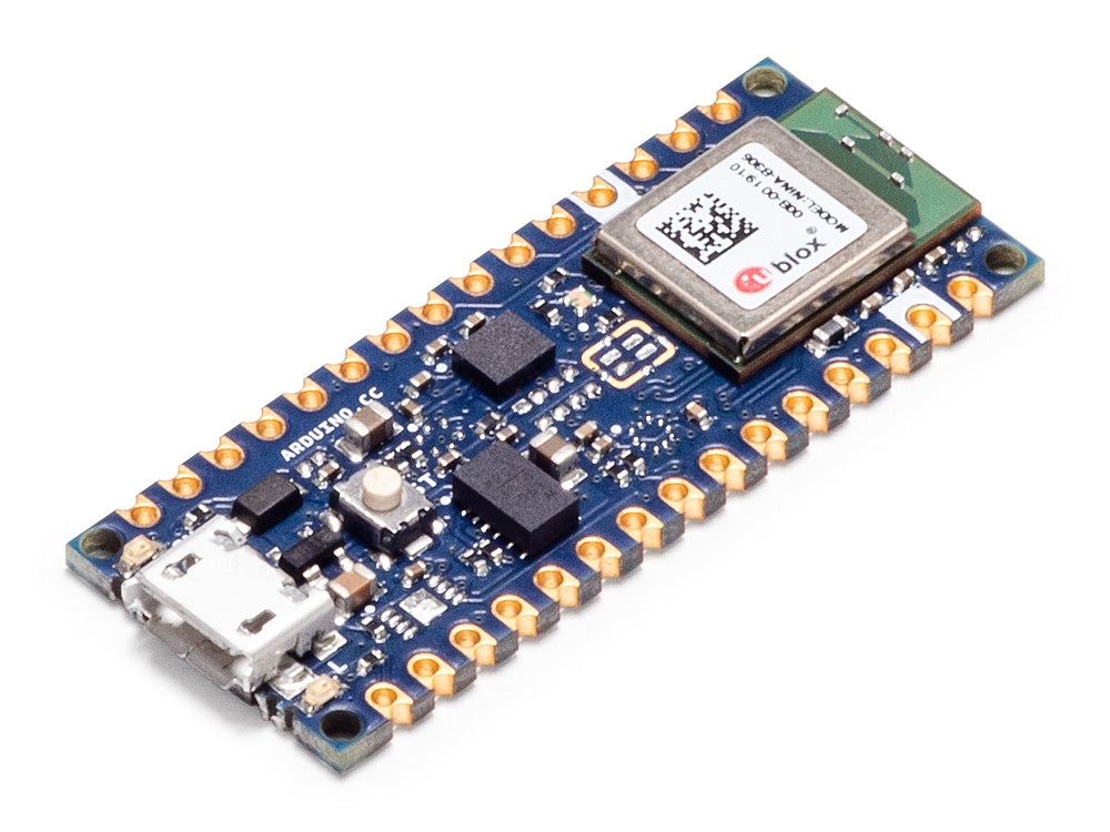
Designed for short range BT interactions and power savvy projects. This compact and reliable Nano board is built around the NINA B306 module, based on Nordic nRF 52840 and containing a powerful Cortex M4F.
Its architecture, fully compatible with Arduino IDE Online and Offline, has a 9 axis Inertial Measurement Unit (IMU) and a reduced power consumption compared to other same size boards.
This allows the design of wearable devices and movement sensing projects that need to communicate to other devices at a close range. Arduino Nano 33 BLE is also ideal for automation projects thanks to the multiprotocol BT 5.0 radio.
Specifications
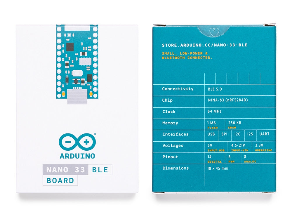
This board is based on the nRF 52840 microcontroller.
| Clock | 64MHz |
| Flash | 1MB |
| RAM | 256KB |
Please note: Arduino Nano 33 BLE only supports 3.3V I/Os and is NOT 5V tolerant so please make sure you are not directly connecting 5V signals to this board or it will be damaged. Also, as opposed to Arduino Nano boards that support 5V operation, the 5V pin does NOT supply voltage but is rather connected, through a jumper, to the USB power input.
To avoid such risk with existing projects, where you should be able to pull out a Nano and replace it with the new Nano 33 BLE, we have the 5V pin on the header, positioned between RST and A7 that is not connected as default factory setting. This means that if you have a design that takes 5V from that pin, it won’t work immediately, as a precaution we put in place to draw your attention to the 3.3V compliance on digital and analog inputs.
5V on that pin is available only when two conditions are met: you make a solder bridge on the two pads marked as VUSB and you power the NANO 33 IoT through the USB port. If you power the board from the VIN pin, you won’t get any regulated 5V and therefore even if you do the solder bridge, nothing will come out of that 5V pin. The 3.3V, on the other hand, is always available and supports enough current to drive your sensors. Please make your designs so that sensors and actuators are driven with 3.3V and work with 3.3V digital IO levels. 5V is now an option for many modules and 3.3V is becoming the standard voltage for electronic ICs.
The Bluetooth is managed by a NINA B306 module.
The IMU is a LSM9DS1 and it is managed through I2C.
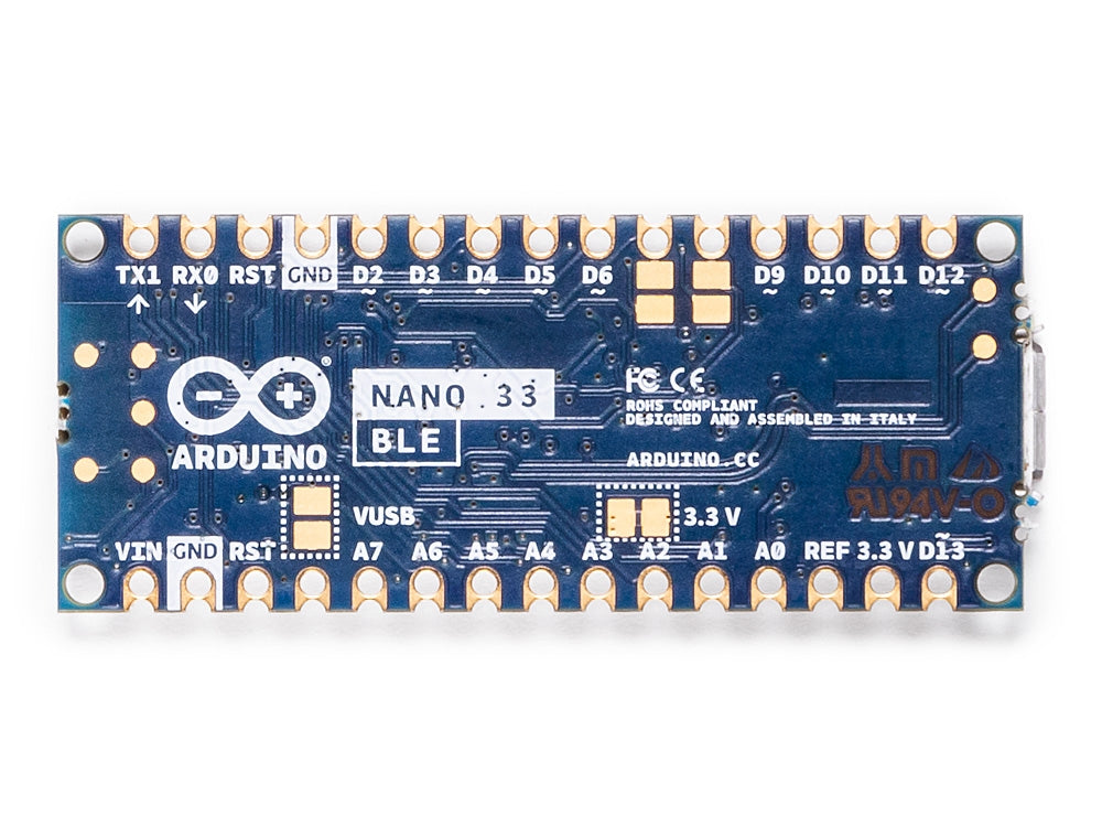
The board has a two 15 pins connectors - one on each side -, pin to pin compatible with the original Arduino Nano.
| Pin | Funcion | Type | Description |
| 1 | D13/SCK | Digital | SPI SCK; GPIO |
| 2 | +3V3 | Power Out | Internally generated power output to external devices |
| 3 | AREF | Analog | Analog Reference; can be used as GPIO |
| 4 | A0 | Analog | ADC in; can be used as GPIO |
| 5 | A1 | Analog | ADC in; can be used as GPIO |
| 6 | A2 | Analog | ADC in; can be used as GPIO |
| 7 | A3 | Analog | ADC in; can be used as GPIO |
| 8 | A4/SDA | Analog | ADC in; I2C SDA; Can be used as GPIO (*) |
| 9 | A5/SCL | Analog | ADC in; I2C SCL; Can be used as GPIO(*) |
| 10 | A6 | Analog | ADC in; can be used as GPIO |
| 11 | A7 | Analog | ADC in; can be used as GPIO |
| 12 | VUSB | Power In/Out | Normally NC; can be connected to VUSB pin of the USB connector by shorting a jumper |
| 13 | RST | Digital In | Active low reset input (duplicate of pin 18) |
| 14 | GND | Power | Power Ground |
| 15 | VIN | Power In | Vin Power input |
| 16 | TX | Digital | USART TX; can be used as GPIO |
| 17 | RX | Digital | USART RX; can be used as GPIO |
| 18 | RST | Digital | Active low reset input (duplicate of pin 13) |
| 19 | GND | Power | Power Ground |
| 20 | D2 | Digital | GPIO |
| 21 | D3/PWM | Digital | GPIO; can be used as PWM |
| 22 | D4 | Digital | GPIO |
| 23 | D5/PWM | Digital | GPIO; can be used as PWM |
| 24 | D6/PWM | Digital | GPIO; can be used as PWM |
| 25 | D7 | Digital | GPIO |
| 26 | D8 | Digital | GPIO |
| 27 | D9/PWM | Digital | GPIO; can be used as PWM |
| 28 | D10/PWM | Digital | GPIO; can be used as PWM |
| 29 | D11/MOSI | Digital | SPI MOSI; can be used as GPIO |
| 30 | D12/MISO | Digital | SPI MISO; can be used as GPIO |
(*) As opposed to other Arduino Nano boards, pins A4 and A5 have an internal pull up and default to be used as an I2C Bus so usage as analog inputs is not recommended. Opposed to Arduino Nano boards that support 5V operation, the 5V pin does NOT supply voltage but is rather connected, through a jumper, to the USB power input.
On the bottom side of the board, under the communication module, debug signals are arranged as 3x2 test pads with 100 mil pitch. Pin 1 is the bottom left one with the USB connector on the left and the test pads on the right.
| Pin | Function | Type | Description |
| 1 | +3V3 | Power Out | Internally generated power output to be used as voltage reference |
| 2 | SWD | Digital | nRF52480 Single Wire Debug Data |
| 3 | SWCLK | Digital In | nRF52480 Single Wire Debug Clock |
| 5 | GND | Power | Power Ground |
| 6 | RST | Digital In | Active low reset input |
Downloads